Dld Circuit Diagram
Dld circuit combinational Schematic illustrations of the simulated dld system: (a) dld array with Digital clock circuit diagram using 4026
Schematic illustrations of the simulated DLD system: (a) DLD array with
4 bit up counter Dld application circuits Dld circuit equation
Dld full adder circuit board work
Multisim dldDld flip project flop digital logic counter bit using ic timer Dld simulated array systemCircuit diagram logic password security system multisim gate dld project.
Adjustable constant current laser diode/led driverPassword security system on multisim Dld projectLaser driver diode current constant led adjustable schematic drive electronics lab dc sch.

Dld adder circuit board
Clock digital circuit using diagram dld segment hours minutes alarm display button displays source .
.


PASSWORD SECURITY SYSTEM ON MULTISIM | PROJECT | CIRCUIT DIAGRAM

4 Bit Up Counter | using D Flip Flop | Digital Logic Design | DLD Demo

Dld Project - Multisim Live

DLD Application Circuits | Electronic Circuits | Amplifier
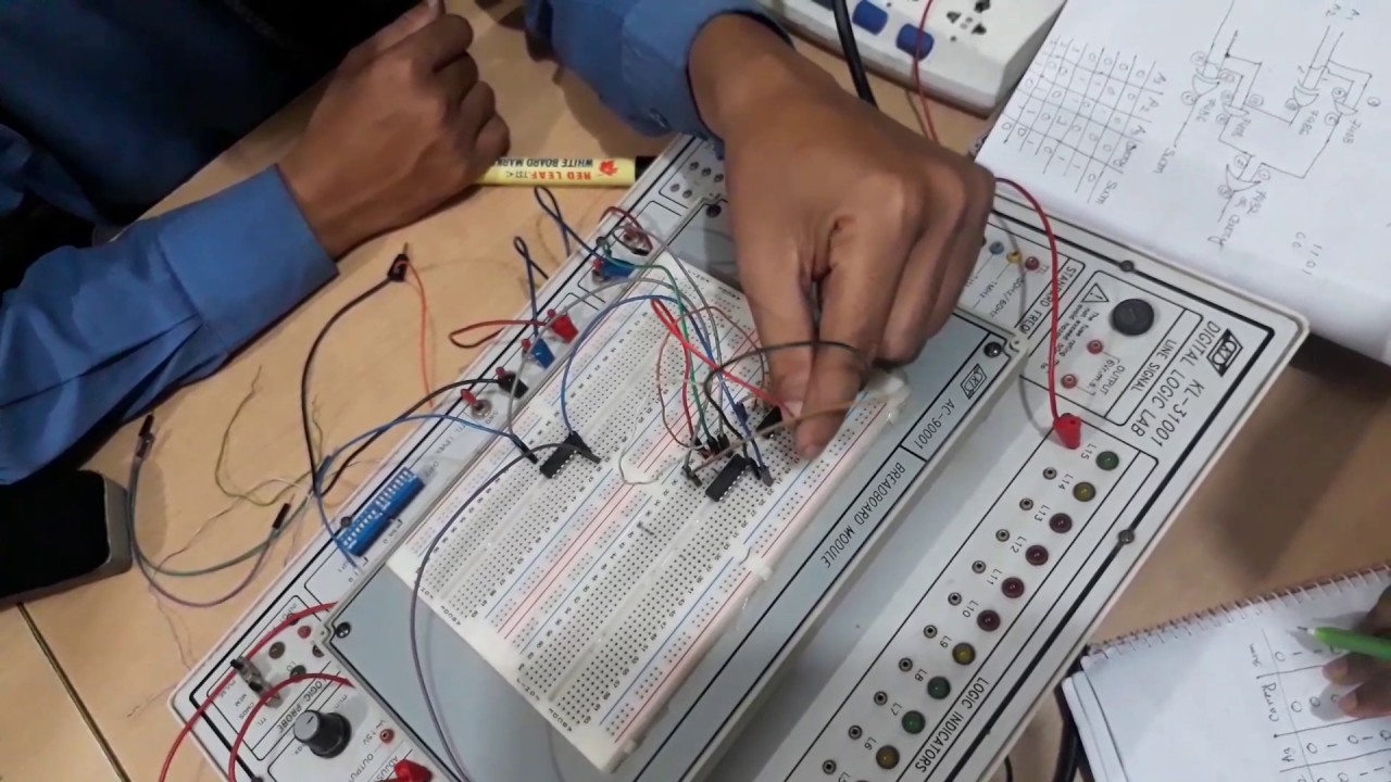
DLD Full adder Circuit board work - YouTube

DLD | EQUATION TO CIRCUIT DESIGN (PRACTICE EXAMPLES) - YouTube

Schematic illustrations of the simulated DLD system: (a) DLD array with

DLD | COMBINATIONAL CIRCUIT ANALYSIS and EQUATION TO CIRCUIT DESIGN